
Digital Logic Lab Trainer EE-33000Description
- Description
Description
The EE-33000 Digital Logic Lab Trainer is a comprehensive and self-contained system suitable for digital logic experiments. All necessary equipment for experiments such as power supply, signal generator, switches and displays and installed on the main unit. The 11 experiments modules cover wide variety of essential topics in the field of digital logic. It is a time and cost saving trainer for both student and engineers interested in developing and testing digital logic circuit prototypes.
Features
• Suitable for basic logic gate, combinational / assembled logic, sequential logic, and microprocessor circuit experimentation and design.
• Ideal tool for learning the basics of digital logic circuits.
• Integrated training system, with complete curriculum.
• Comprehensive power supply, signal supply, and testing devices for convenient experimentation.
• Complete with Computer Interface : Serial Interface, Centronic Interface & USB Interface
• 50MHz Auto Ranging Frequency Counter
• Digital DC Voltmeter
• Expandability and flexibility of experiments greatly increased by large breadboard.
• Use with TTL, CMOS, NMOS, PMOS and ECL circuits.
• All supplies equipped with overload protection.
Main Unit DLLT-1300
Fixed DC Power Supply Voltage range: +5V, -5V, +12V and -12V
Maximum current output: 1A for +5V rail, 300mA for others
Output overload protection
Variable DC Power Supply Voltage range: +1.5V ~ +22V, -1.5V ~ -22V
Maximum current output: 0.5A
Output overload protection
Variable Clock Generator Six frequency ranges:
1Hz to 10Hz
10Hz to 100Hz
100Hz to 1kHz
1kHz to 10kHz
10kHz to 100kHz
100kHz to 1MHz
Output level: independent and simultaneous TTL and CMOS, CMOS output range adjustable from +1.5V to +15V
Preset Frequency Generator Preset frequencies:
1Hz
50/60Hz
1MHz with accuracy of ±0.01% at 1MHz
Output level: independent and simultaneous TTL and CMOS, CMOS output range adjustable from +1.5V to +15V
Line Signal Generator 50/60Hz
Output Voltage: 6V rms
Data Switches Two 8-bit DIP switches giving 16-bit TTL level output
Four toggle switches, each with debounce circuit, TTL and CMOS outputs
Pulser Switches Two sets, each having debounced TTL and CMOS, Q and /Q outputs and pulse width of more than 5ms, Fan-Out: 10 TTL Loads
Thumbwheel Switches Two-digit, BCD code output, common point input
Logic Indicators 16 sets of independent LEDs, indicating high and low logic states
Input impedance: <100kW
Seven-Segment Displays Four sets of independent 7-segment displays, with BCD, 7-segment decoder/driver and decimal point input terminal, input with 8-4-2-1 code
Logic Probe TTL and CMOS level, 3mm LED displays indicate high and low logic states
Computer Interface Serial Interface, Centronics Interface & USB Interface
Frequency Counter 50MHz Auto Ranging Frequency Counter
Digital DC Voltmeter 4 Digits LED display
Four voltage ranges :
0V to 199.9VDC
0V to 19.99VDC
0V to 1.999VDC
0V to 199.9mVDC
Input Impedance: 10Mohm for any range
Speaker 8W, 0.25W speaker with driver circuit
Solderless Breadboard 1680 interconnected tie points, accepting all DIP devices, components with leads and solid wires of AWG #22-30 (0.3mm to 0.8mm)
Accessories Power lead, connecting leads and user manual
Power Supply 240V AC ±10% 50/60Hz
Physical Characteristics
(Main Unit) Dimensions: 465mm (width), 330mm (depth), 150mm (height)
Weight: 6kg
Physical Characteristics
(Experiments Modules) Dimensions: 265mm (width), 200mm (depth), 50mm (height)
Weight : 1.5kg each
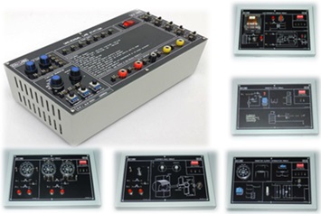
EE-33000 Experiment Modules
Eleven units experiments modules form the basis for over 60 experiments detailed in the comprehensive experiment manual. Each module contains the experiment circuit which is clearly illustrated by a circuit diagram on its top panel. Switch faults are also incorporated into the modules for simulating fault situations.
Features
• All 11 experiment modules equipped with an 8-bit DIP switch for fault simulation. Users learn how to solve various problems by setting the DIP switch to different positions.
• Solutions or model answer for all failure test are listed in the experiment manual for user’s reference.
• 2mm stackable test leads set used throughout the main unit and all experiment modules.
• Comprehensive experiment manual and instructor’s manual.
• Experiment module dimension 255 x 165 x 30mm
Experiment Modules
Eleven modules form the basis for over 60 experiments detailed in the comprehensive experiment manual. Each module contains the experiment circuit which is clearly illustrated by a circuit diagram on its top panel. Switch faults are also incorporated into the modules for simulating fault situations.
Experiments Module 01: Basic Logic Gates Experiment Module
Experiments Module 02: Assembled Logic Circuits (1) Experiment Module
Experiments Module 03: Assembled Logic Circuits (2) Experiment Module
Experiments Module 04: Assembled Logic Circuits (3) Experiment Module
Experiments Module 05: Assembled Logic Circuits (4) Experiment Module
Experiments Module 06: Assembled Logic Circuits (5) Experiment Module
Experiments Module 07: Clock Generator Circuit Experiment Module
Experiments Module 08: Sequential Logic Circuits (1) Experiment Module
Experiments Module 09: Sequential Logic Circuits (2) Experiment Module
Experiments Module 10: Memory Circuits (1) Experiment Module
Experiments Module 11: Memory Circuits (2) Experiment Module
The full list of experiments performed using the above modules and detailed in the experiment manual are:
1. Basic Logic Gates Experiments
1. Introduction to logic and switches
2. Logic gates circuit experiments
a. Diode Logic (DL) circuit
b. Resistor-Transistor Logic (RTL) circuit
c. Diode-Transistor Logic (DTL) circuit
d. Transistor-Transistor Logic (TTL) circuit
e. CMOS Logic circuit
3. Threshold Voltage measurement experiments
a. TTL logic circuit
b. CMOS logic circuit
4. Voltage/current measurement experiments
a. TTL I/O Voltage/current output measurement
b. CMOS I/O Voltage/current output measurement
5. Basic logic gate transmission delay measurements
a. TTL logic gate transmission delay measurements
b. Schmitt gate transmission delay measurements
c. CMOS logic gate transmission delay measurements
6. Basic logic gate characteristics
a. AND gate characteristics
b. OR gate characteristics
c. NOT gate characteristics
d. NAND gate characteristics
e. NOR gate characteristics
f. XOR gate characteristics
7. Interfacing between logic gates
a. TTL to CMOS interface
b. CMOS to TTL interface
2. Combination / Assembled Logic Circuits Experiments
1. NOR gate circuit experiment
2. NAND gate circuit experiment
3. XOR gate circuit experiment
a. with NAND gate
b. with basic equations
4. A-0-1 gate circuit experiment
5. Comparator circuit experiments
a. with basic logic gates
b. with TTL comparator IC
6. Schmitt gate circuit experiment
7. Open collector gate circuit experiment
a. High Voltage/current driver circuit
b. Constructing an AND gate with open collector gate
8. Three-state gate circuit experiments
a. Truth table experiment
b. Constructing an AND gate with three-state gate
c. Bidirectional transmission circuit
9. Half adder and full adder experiments
a. with basic logic gates
b. Full adder circuit
c. High-speed adder carrier generator
d. BCD code adder circuit
10. Half subtractor and full subtractor experiments
a. with basic logic gates
b. with full adder and inverter circuit
11. Arithmetic Logic Unit (ALU) circuit experiment
12. Bit parity generator experiments
a. with XOR gate
b. with bit parity generator IC
13. Encoder circuit experiments
a. Constructing a 4 to 2-bit encoder with basic logic gates
b. Constructing a 10 to 4-bit encoder with TTL IC
14. Decoder circuit experiments
a. Constructing a 4 to 2-bit decoder with basic logic gates
b. Constructing a 10 to 4-bit decoder with TTL IC
c. Decoding a 7-segment display with BCD code
15. Multiplexer circuit experiments
a. Constructing a 2 to 1-bit multiplexer with basic logic gates
b. Using a multiplexer to create functions
c. Constructing an 8 to 1-bit multiplexer with TTL IC
16. Demultiplexer circuit experiments
a. Constructing a 1 to 2-bit demultiplexer with basic logic gates
b. Constructing a 1 to 8-bit demultiplexer with CMOS IC
17. Digitally controlled analogue multiplexer/demultiplexer circuits
a. Characteristics of analogue switches
b. Bidirectional transmission with CMOS IC analogue switches
3. Clock Generator Circuit Experiments
1. Constructing an oscillator circuit with basic logic gates
2. Constructing an oscillator circuit with Schmitt gate
3. Voltage Controlled Oscillator (VCO) circuit
4. 555 IC oscillator circuit experiments
a. 555 oscillator circuit
b. Voltage controlled oscillator circuit
5. Monostable multivibrator circuit experiments
a. Low-speed monostable multivibrator cicuits
a-1. Non-retriggerable circuit
a-2. Retriggerable circuit
b. High-speed monostable multivibrator cicuits
b-1. Non-retriggerable circuit
b-2. Retriggerable circuit
c. Constructing a monostable multivibrator with 555 trigger
d. Constructing a non-retriggerable circuit with TTL IC
e. Constructing a retriggerable circuit with TTL IC
f. Constructing a variable duty cycle oscillator circuit with monostable multivibrator
4. Sequential Logic Circuits Experiments
1. Constructing an R-S flip-flop with basic logic gates
2. Constructing a D flip-flop with an R-S flip-flop
3. Constructing a T flip-flop with a D flip-flop
4. Constructing a J-K flip-flop with an R-S flip-flop
5. Constructing a shift register with a D flip-flop
a. Serial-in serial-out shift register
b. Serial-in parallel-out shift register
c. Parallel-in serial-out shift register
d. Parallel-in parallel-out shift register
6. Preset left/right shift register circuit experiment
7. Noise elimination circuit with R-S flip-flop
8. Constructing counters with J-K flip-flop
a. Asynchronous binary up-counter circuit
b. Asynchronous decimal up-counter circuit
c. Asynchronous divide-by-N up-counter circuit
d. Asynchronous binary down-counter circuit
e. Synchronous binary up-counter circuit
f. Synchronous binary up/down counter circuit
g. Preset synchronous binary up/down counter circuit
h. Preset synchronous decimal up/down counter circuit
i. Ring counter circuit
j. Johnson’s counter circuit
5. Memory Circuit Experiments
1. Constructing Read Only Memory (ROM) with diodes
2. Constructing Random Access Memory (RAM) with D flip-flops
3. 64-bit RAM circuit
4. Erasable Programmable Read Only Memory (EPROM) circuit
5. Electronically Erasable Programmable Read Only Memory (EEPROM) circuit
6. Constructing a dynamic scanning counter with a single-chip microprocessor
EE-33000 Accessories
1. 2mm Stackable Test Leads Sets: 2mm-2mm, 300mm (L) x 25 Pcs (5 Color Coded: Red, Yellow, Blue, Green & Black)
2. CD softcopy Format: Instructional Experiments and Experiments Manual
3. Power Cord (UK 3 Pin)
Note: Due to products continuous development process, layout and specification may change without prior notices.